10 KiB
Project Structure
- doc Contains all relevant documentation needed for this project
- download Contains various files downloaded for this project
- corebundle-mst_lab.zip First version of Custom Xillybus IP Core implementation generated by "IP Core Factory"
xillybus_debug: Upstream, 32-bits, 256 B/s, General Purposexillybus_config: Downstream, 16-bits, 204.8 kB/s, Address/Data Interface (16 address bits)xillybus_audio: Upstream/Downstream, 32-bits, 204.8 kB/s, Data acquisition/Playbackxillybus_smb: Upstream/Downstream, 8-bits, 10.24 kB/s, Command and Status
- corebundle-mst_lab2.zip Second version of Custom Xillybus IP Core implementation generated by "IP Core Factory". Currently in use
xillybus_debug: Upstream, 32-bits, 256 B/s, General Purposexillybus_config: Downstream, 32-bits, 204.8 kB/s, Address/Data Interface (16 address bits)xillybus_audio: Upstream/Downstream, 32-bits, 204.8 kB/s, Data acquisition/Playbackxillybus_smb: Upstream/Downstream, 8-bits, 10.24 kB/s, Command and Status
- CypressDriverInstaller_1.exe Windows drivers for zedboard USB-UART
- xillinux-2.0.img.gz Xillinux SD Card image
- xillinux-eval-zedboard-2.0c.zip Zedboard Xillybus demo project
- corebundle-mst_lab.zip First version of Custom Xillybus IP Core implementation generated by "IP Core Factory"
- modelsim Contains .do files for modelsim simulation
- src Constains the actual vhdl source files for this project
- sim Contains the simulation testbenches
- UNUSED Contains (partially) implemented logic that is not used in the final version
- sw Contains the software that allows to communicate with the FPGA logic from Linux through the Xillybus API
- syn Contains a zedboard Vivado test project used to test various parts of the VHDL implementation
- xillinux-syn Contains the final Vivado project implementing the xillybus IP core, ZYNQ System, and instantiating our FPGA logic. This is a modified version of the xillybus-demo project
- vivado Contains the actual Vivado Project file
- vhdl/src Cotains the project top entity (
xillydemo.vhd). The FPGA logic in instantiated in this file - The rest of the directories are taken verbatim from the demo project and are necessary for all the peripheral components used by xillinux.
Board Mapping
| Zedboard Pin | Description |
|---|---|
| JC1 PMOD Connector (Upper Row) | PMOD-AD1 Board |
| JD1 PMOD Connector (Upper Row) | PMOD-DA3 Board |
| JA1 PMOD JA4 Pin | (Optional) External Clock [NOTE: Clk has to be connected in VHDL and PLL has to be reconfigured accordingly] |
| JA1 PMOD JA1 Pin | External SYNC Pulse [NOTE: if pin is left unconnected (floating), it will register as a pulse] |
| SW7 | Standby / Operation Mode (Allows xillinux to write configuration if in Standby Mode) |
| LED7 | Standby Mode Status (ON if FPGA in Standby Mode) |
| LED6 | Sync Status (ON if Sync Pulse was registered) |
| BTNC | Global reset |
| BTNU | Debug value reset |
Project Description
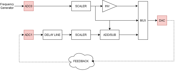
This project implements the above feedback loop in FPGA logic. The components of the feedback loop are detailed below:
- ADC The ADC (PMOD-AD1) is capable of operating at a maximum frequency of 20 MHz, and converting an analog signal every 18 clock cycles (ca 1.1 MHz Sampling Frequency). All PMOD Connectors on the Zedboard are fixed to 3.3V, hence the ADC can convert analog signals in the range 0V-3.3V to 12-bits.
- DAC The DAC (PMOD-DA3) is capable of operating at a maximum frequency of 50 MHz, and converting a digital signal every 16 clock cycles (ca 1.25 MHz). The DAC uses an internal 2.5 V Voltage reference (uncorrelated to the used VCC Voltage), and can thus convert 16-bits to 0V-2.5V.
- DELAY LINE The delay line allows to delay the converted ADC values by a pre-specified amount of clock cycles.
- SCALER The scaler allows the converted ADC values to be scaled. It uses a 5-bit multiplication factor that is intepreted as a Q1.4 (1-Bit Integer, 4-Bit Fractional) fixed point number. The signals are scaled with respect to the configured Bias Offset. Note that when scaling up the signal may be capped due to overflow conditions in the internal representation. See Overflow Considerations
e.g. A value of 16(decimal) is intepreted as scaling by 1, a value of 15(decimal) is intepreted as scaling by 0.9375, and a value of 24(decimal) is is intepreted as scaling by 1.5. - ADD/SUB The ADD/SUB allows to either add or subtract the input signals (Sig0 +/- Sig1).
- INV The INV inverts the input signal 0. The negated signal 0 is used if the loop is in Single Input Mode configured as Negative Feedback.
- MUX The MUX selects between the signals, allowing either input signal 0 passthrough, or feedback result to be outputted.
Timing Considerations
The whole system is clocked at 20 MHz (highest supported frequency of ADC).
The logic between the ADC and DAC is implemented in a 2-stage pipeline format, so that the whole feedback loop follows the 18 clock cycle cadence of the ADC.
Bias Offset
Because both the used ADC and DAC are unipolar, signals have to be biased accordingly on input and output. In order to have correct processing of biased signals, the bias offset has to be configured in the typedef_package. The default configured bias is 2048 (1.65V), and is in the middle of the ADC input range.
Input/Output Voltage Range
Because the input range is 0-3.3V but the output range is 0-2.5V, the output signal amplitude is approx. 75% of the input signal amplitude when using a scaling of 1 (16 in config). In order to compensate for that you have to scale by a factor of 1.32 (21 in config). Note that when using the factor 1.32 to compensate this reduces the effective input range to 0.4-2.9V (with default bias).
Overflow Considerations
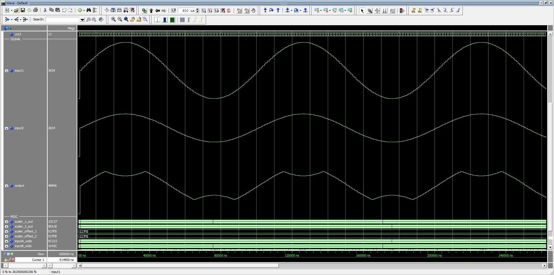
Due to the internal representation signals may be capped to their maximum value in-between arithmetic operations, leading to unwanted signal distortion in the output. The user has to take into account that no signal is exceeding the output voltage range.
e.g. The below simulation shows a negative feedback loop, where Input 2 is scaled by 1 and subtracted by Input 1 scaled by 1.32. Because the scaling of Input 1 is capped before the subtraction of Input 2 we get an unwanted distortion.
USAGE
Preperation
- Write the image contained in
download/xillinux-2.0.img.gzto the SD card. - Copy the files in the
xillinux-syn/bootfilesdirectory into the first partition of the SD Card - Open the Vivado Project under
xillinux-syn/vivado/xillydemo.xprand generate the Bitstreamfile - Copy the Bitstreamfile into the first partition of the SD Card
- Follow the instruction in Chapter 4 of
doc/Xillybus/xillybus_getting_started_zynq.pdfto set the correct switch/jumper positions - Connect SD Card to Zedboard
- Connect the USB cable to the UART port. The UART uses the 8N1 format and a baudrate of 115200.
- Optionally you can also connect VGA monitor, audio, keyboard/mouse (using USB-OTG), as the xillinux is a fully fledged Linux OS.
Boot
The UART should automatically connect to a root shell (after U-Boot did it's thing). The root user has no password set.
The system should be halted (using the halt or shutdown now command) before powering off the board, to prevent SD Card corruption.
Configuration
The FPGA logic contains a configuration memory with a pre-defined (changable in typedef_package.vhd) number of configuration "slots". Each slot contains the configuration for the feedback loop (Delay Line clock count, scaler factor, add/sub selection, MUX selection), and a timestamp. The timestamp defines the number of clock cycles from the rising edge of the SYNC pulse signal after which the configuration described by the slot is applied. It makes sense for the first configuration slot to have a timestamp of 0. The slots are processed in write order, and not in timestamp order. (Thus slots should have increasing timestamp values).
NOTE: It is valid for a configuration slot to have a timestamp lower than the previous. The slot will be applied for at least 1 clock cycle before the next slot can be applied.
The xillybus_config linux device file is used to write to the configuration memory of the FPGA. Note that the standby switch has to be enabled (Standby status led on) in order to write the configuration to the FPGA. As long as the standby switch is enabled, the feedback loop is held in reset.
The write_config.c C program can be used to write the configuration onto the FPGA.
e.g. ./write_config config /dev/xillybus_config
Config File
Each line of this file defines a configuration slot and consists of integer numbers delimited by white spaces in the following order:
ADDSUB_MODE ADD_INPUT_MUX DELAY FACTOR0 FACTOR1 TIMESTAMP
- ADDSUB_MODE: Select feedback mode (0=Negative, 1=Positive)
- ADD_INPUT_MUX: Select feedback input (0=Single Input Mode [ADC0], 1=Double Input Mode)
- DELAY: Clock cycles counts (50 ns period) to delay the feedback signal [0-65535]
- FACTOR0: Multiplication factor to apply to the ADC Signal0 [0-32] (NOTE: Integer is intepreted as a Q1.4 Fixed Point Number!)
- FACTOR1: Multiplication factor to apply to the ADC Signal1 [0-32] (NOTE: Integer is intepreted as a Q1.4 Fixed Point Number!)
- TIMESTAMP: Defines the clock count number from the sync pulse from which on the configurations settings will be applied. [32-bit unsigned integer]
NOTE: In Single Input Mode the feedback mode (Positive/Negative) selects if the input signal 0 is passed through as is, or negated.
Debug
The FPGA logic allows debug values to be sent to the Linux via the xillybus_debug device file.
Currently the FPGA logic sends every second the max values of the both ADC channels, Scaler output, and DAC. The max values can be externally reset (see Mapping).
The read_debug.c C program can be used to read the debug values. Since the program enters an endless loop, a signal handler has beeen implemented and the program can be safely terminated with CTRL-C & CO.
e.g. ./read_debug /dev/xillybus_debug

